Semiconductor definitions/descriptions

Intrinsic and Extrinsic Semiconductors

Intrinsic

Intrinsic semiconductors are pure and undoped. They have an equal number of conduction electrons and holes. Thermal excitation is required for conduction.

Extrinsic

Extrinsic semiconductors are doped with impurity atoms, which generate majority carriers. The type of majority carrier is dependent on the dopant used. These are as follows:

N-type- Majority carriers are electrons, minority carriers and holes.

P-type- Majority carriers are holes, minority carriers and electrons.


Drift velocity of carriers

Drift velocity is the average velocity that a charge carrier, such as an electron, attains in a material due to an electric field.


Band-gap energy

The band-gap energy is the energy required to move an electron from the valence band to the conduction band.


Electron-hole recombination and the frequency of light emitted by an LED.

Electron-hole recombination

When an electron which has previously been excited from the valence, to the conduction band, falls back into an empty state in the valence band.

Frequency of light emitted by an LED

When an electron moves back from the conduction band to the valence band, energy equal to the band-gap energy is emitted.

This energy produces a frequency which is equal to the band-gap energy divided by Planck’s constant. In LEDs, the frequency produced is in the form of light (Hence the name Light Emitting Diode).

Advertisement

Semiconductors

Overview

As the name suggests semiconductors are partially conductive materials, and lay somewhere between the conductivity of conductive metals and insulators.

N-type semiconductors

N-type semiconductors are generally composed of silicon, or germanium, doped in antimony. The doping provides a  free electron which increases the conductivity of the material.

The name derives from negative charge. This is because of electric current, where electrons break free from their atoms, and create a direction flow of electrons, with the aid of an electric field. Electrons flow towards vacancies in positively biased materials.

P-type semiconductors

P-type semiconductors are also generally composed of silicon, or germanium. However, Instead of being doped in antimony, they are doped in an element such as indium. This has the opposite effect to that of doping in antimony, as indium has a vacancy in its outer shell of electrons, to which a free electron can easily occupy.

The letter ‘P’ represents the fact that this material has a positive charge.

Conclusion

Under normal circumstances, In N-type semiconductors free electrons flow away from the materiel. Whereas In P-type semiconductors, free electrons flow towards the material to occupy the vacancies.

In terms of conventional current, current flows from P-type (positive) semiconductors, and current flows towards N-type (negative) semiconductors.

Diode bridge

Overview

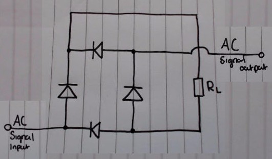
This is a diode bridge. It converts alternating current (AC), into direct current (DC). The circuit is set up so that current is always flowing towards the input of RL, and away from the output. More information about the properties of diode can be found here:’https://tphelectronics.com/2015/09/29/diodes/

ddone

AC signal output is most commonly just connect to ground (0v).

RL represents the circuit to which you’re applying the DC voltage.


Signal diagram explanation

dAC

This shows one full oscillation of the AC signal at the input. Whilst the signal is above the horizontal line, the voltage at the signal input is positive. Whilst the signal is below the horizontal line, the signal input is positive


Flow of current during positive half of the oscillation.

dACp

During the section labelled ‘Input is positive’, here’s how the current flows around the circuit:

dbp

The reason why the current can’t flow through D4, after passing through RL, is because D4 has already been reverse biased by current flowing from the AC input.


Flow of current during negative half of the oscillation.

dACn

During the section labelled ‘Input is negative’, here’s how the current flows around the circuit:

dbn


Conclusion.

As you can see, regardless of whether the AC input is positive or negative, the current flowing through RL never changes. If we could see what the current looked like at RL, It’d look something like this:

dCRL


Notes for future.

I’ll add in a diagram and explanation as to how to dampen the rippling effect seen in the graph above.

Bipolar Junction Transistors (BJTs)

BJT overview

BJTs (Bipolar Junction Transistors) can either be of one of two types, NPN or PNP. This refers to the polarity of the materials used in them. ‘N’ means that the layer of material has a negative polarity, and ‘P’ means that is positive.

This is where BJTs get their name from, Bipolar references the fact that it consists of two types of semiconductor (N and P). Junction refers to the fact that there is a physical connection between these semiconducting materials, as opposed to a Field Effect Transistor.

The NPN/PNP material arrangement on BJTs corresponds to the terminals of the transistor. Collector, Base, and Emitter. In an NPN transistor, the collector and the emitter terminals are connected to a semiconducting material with a negative polarity, and the Base a positive. Whereas PNP transistors are the opposite. More information about P and N type semiconductors can be found here: ‘https://tphelectronics.com/2016/09/30/semiconductors/‘.


NPN bipolar junction transistor

When current enters B (the Base) , It allows current to flow from C (the Collector) to the E (the Emitter). This is shown by the direction of the arrow in the schematic. When there is no current applied to B, current cannot flow from C to E.

In an NPN transistor there is a PN junction between the base and the emitter terminals. So, as within diodes, there is around a 0.7v drop between the base and the emitter when it is turned on. Therefore, for a significant amount of current to be able to flow from C to E, the base needs to be above 0.7v.

Depending on the type of NPN BJT, the current flowing from the emitter is around 100x that of the current flowing into the base. Of course for this to happen, the collector needs to be able to draw that amount of current from the source.

The current flowing out of the emitter is always equal to the sum of the current flowing from the base and the collector.

npn-bjt


PNP bipolar junction transistor

PNP BJTs work in the opposite way to NPN BJTs. When the base is 0.7v less than that of the emitter, current is able to flow in through the emitter, and out through the collector. This however limits the components usage, as the voltage at the base always needs to be below that of the emitter. In addition to this, using the circuit arrangement: ‘not gate using a transistor‘, an NPN transistor can be set up to perform the same operation.

PNP transistors are mainly used in conjunction with complimentary NPN transistors, circuits like push-pull amplifiers.

pnp-bjt

Diodes

Overview

A diode is a semiconductor which has two terminals: an anode and a cathode. They are composed of two layers of semiconducting material, one side doped to make it an N-type semiconductor, and the other doped to make it a P-type semiconductor. The anode is on the side of the P-type, and the cathode is on the side of the N-type.(More information about types of semiconductors can be found here: ‘https://tphelectronics.com/2016/09/30/semiconductors/‘).

One of the main characteristics of diodes is that they only allow current to flow in one direction. This means that they can be used to filter out alternating current, or even rectify it with the use of a diode bridge.


Configurations

They’re used both in forward bias, and reverse bias. This refers to the direction in which current flows (forward being anode to cathode, and reverse being cathode to anode).

When forward biased no current flows through the diode until more than the minimum voltage is applied (This is because of the depletion region). This means that it can be used to filter out voltages below this value (e.g noise). The value itself is dependent on the type of diode.

When reverse biased only a few nanoamps flow through the diode.However, If the voltage applied is too large, it’ll cause the diode to breakdown. In most cases this will destroy the diode, but the breakdown in zener diodes do not destroy it (this is used to regulate voltage).

diode-diagram-label