Introduction to operational amplifiers

Practical op amp model

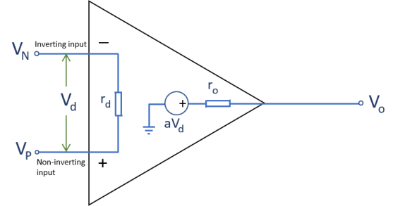
Practical operation amplifier model.

Key-part_1

Key-part_2


In an ideal operational amplifier (op amp), the value of rd is considered to be infinite when in actual fact the resistance is around 10MΩ. This value is dependent on the variety of omp amp and generally increases with price. The higher the value of rd, the better.

This same premise also applies to the open-loop gain. It’s value in an ideal op amp is also considered to be infinite, when in actual fact it is around 10M.

ro however is the inverse, as in an ideal op amp it is 0Ω and a typical practical value is about 10Ω,


Vout_formula

Using the above formula the following can be derived:

V difference formula

The difference between the voltage on the inverting input and the non-inverting input is equal to the output voltage divided by the gain.

Now assuming ideal values for the gain (infinite), its value can substituted in and the formula can be rearranged.

V difference formula (values)

Any value divided by infinity is equal to zero, therefore:

V difference formula (simp)

Looking back at the original formula, the following can be deduced:

Vout_formula (2)

Vout_formula (3)

Substitute in the value for Vd:

Vout_formula (4)

Rearrange:

Vout_formula (5)


In addition to this, two more values can be stated when using ideal values.

The value of rd is infinite, therefore no current is flowing into the inverting or non-inverting terminals (Ip = 0A and In = 0A).

The output impedance is 0Ω.


Advertisement

Diode bridge

Overview

This is a diode bridge. It converts alternating current (AC), into direct current (DC). The circuit is set up so that current is always flowing towards the input of RL, and away from the output. More information about the properties of diode can be found here:’https://tphelectronics.com/2015/09/29/diodes/

ddone

AC signal output is most commonly just connect to ground (0v).

RL represents the circuit to which you’re applying the DC voltage.


Signal diagram explanation

dAC

This shows one full oscillation of the AC signal at the input. Whilst the signal is above the horizontal line, the voltage at the signal input is positive. Whilst the signal is below the horizontal line, the signal input is positive


Flow of current during positive half of the oscillation.

dACp

During the section labelled ‘Input is positive’, here’s how the current flows around the circuit:

dbp

The reason why the current can’t flow through D4, after passing through RL, is because D4 has already been reverse biased by current flowing from the AC input.


Flow of current during negative half of the oscillation.

dACn

During the section labelled ‘Input is negative’, here’s how the current flows around the circuit:

dbn


Conclusion.

As you can see, regardless of whether the AC input is positive or negative, the current flowing through RL never changes. If we could see what the current looked like at RL, It’d look something like this:

dCRL


Notes for future.

I’ll add in a diagram and explanation as to how to dampen the rippling effect seen in the graph above.

Potentiometers

Potentiometers are essentially potential dividers with one significant difference. You can variate the voltage that is being outputted. The resistance, and consequently the voltage, can be changed by adjusting the position of the knob. For reference, here’s the link to the post on potential dividers:  ‘https://thelectronicsblog.wordpress.com/2015/11/11/potential-dividers’


potentiometer real view

Above is a diagram of what a potentiometer physically looks like. Rotating the knob directly changes the position of the wiper. The position that the wiper is in dictates the voltage outputted from the wiper wire.

To explain this more easily, imagine that the two resistors from the potential divider diagram have been squished together, and the insulated coating has been removed.

potential-divider1potential-divider pot.jpg

Assume that R1 and R2 in the diagram on the left are each 5k. They have been squished together on the diagram on the right. This forms a 10k piece of resistive material . But because the position of the Vout wire is approximately half way down, it is the same as having a 5k resistors on each side.

potential-divider pot 2

Now assume that the Vout wire is instead now 3/4 of the way down the resistive material. This is equivalent to having a 7.5k resistor as R1, and a 2.5k resistor as R2.

Now that the premise behind potentiometers has been explained, here’s the original physical diagram shown side by side with what the internal wiring of a potentiometer would actually look like:
pot1potentiometer real view


Hopefully you now understand how a potentiometer works. However, if you have any questions, please don’t hesitate to ask.

Bipolar Junction Transistors (BJTs)

BJT overview

BJTs (Bipolar Junction Transistors) can either be of one of two types, NPN or PNP. This refers to the polarity of the materials used in them. ‘N’ means that the layer of material has a negative polarity, and ‘P’ means that is positive.

This is where BJTs get their name from, Bipolar references the fact that it consists of two types of semiconductor (N and P). Junction refers to the fact that there is a physical connection between these semiconducting materials, as opposed to a Field Effect Transistor.

The NPN/PNP material arrangement on BJTs corresponds to the terminals of the transistor. Collector, Base, and Emitter. In an NPN transistor, the collector and the emitter terminals are connected to a semiconducting material with a negative polarity, and the Base a positive. Whereas PNP transistors are the opposite. More information about P and N type semiconductors can be found here: ‘https://tphelectronics.com/2016/09/30/semiconductors/‘.


NPN bipolar junction transistor

When current enters B (the Base) , It allows current to flow from C (the Collector) to the E (the Emitter). This is shown by the direction of the arrow in the schematic. When there is no current applied to B, current cannot flow from C to E.

In an NPN transistor there is a PN junction between the base and the emitter terminals. So, as within diodes, there is around a 0.7v drop between the base and the emitter when it is turned on. Therefore, for a significant amount of current to be able to flow from C to E, the base needs to be above 0.7v.

Depending on the type of NPN BJT, the current flowing from the emitter is around 100x that of the current flowing into the base. Of course for this to happen, the collector needs to be able to draw that amount of current from the source.

The current flowing out of the emitter is always equal to the sum of the current flowing from the base and the collector.

npn-bjt


PNP bipolar junction transistor

PNP BJTs work in the opposite way to NPN BJTs. When the base is 0.7v less than that of the emitter, current is able to flow in through the emitter, and out through the collector. This however limits the components usage, as the voltage at the base always needs to be below that of the emitter. In addition to this, using the circuit arrangement: ‘not gate using a transistor‘, an NPN transistor can be set up to perform the same operation.

PNP transistors are mainly used in conjunction with complimentary NPN transistors, circuits like push-pull amplifiers.

pnp-bjt

Tutorials – Section 1 – Lesson 1 LED Button

Following on from the set-up for this section, we’re going to create a circuit which switches on and off on LED.

For this circuit you will need:

  • An Arduino Board.
  • A piece of breadboard.
  • 1 – 10kΩ resistor.
  • 1 – LED
  • 1 – push button


The anode, cathode, and general orientation of an LED is  shown in a schematic like this:


This is a simple schematic of the circuit.The begging of which will be connected to the 5v rail on the breadboard, and the end will be connected to the ground (GND) rail.

Circ

By pressing in the button in, the LED will light. As soon as the button is no longer being pressed, the light will go off once more.

Here’s the actual circuit shown  below:

rereereerreererrereererre

Tutorials – Section 1 – Setup

For section one we’ll only be using the 5 volts supply pin and the ground pin on the Arduino. Firstly you’ll need to supply power to the Arduino by using the USB cable to either plug it into a computer or another USB socket capable of supplying power.

Once you have done this, connect the Arduino to the breadboard as shown in the diagram below.

section one setup

In the following section 1 tutorials, this same set-up will be used.


Resistor colour codes

resistor

4 Band resistor colour coding

On a resistor which has four bands of color, the first and second bands represent a two digit number. This can be found by looking at which number value the colours represent. In the Figure below, the first band is brown and the second is black. This gives use 10 as our two digit number. Next, you look at the third colour, which represents the multiplier. You take this value and multiply it by the two digit number. In this case, it would be 10 x 100Ω. This would give us a resistor value of 1kΩ.

resistor-colour-coding

Fibre optic cables

Optic fibre cables are comprised of four layers. Data is transferred using beams of light by utilising an effect known as total internal reflection.

optic

Light travels into the glass core, and so long as it is above the critical angle, total internal reflection will occur, causing light to reflect off of the inside of the glass core repeatedly until it reaches the other end.

glass