Bipolar Junction Transistors (BJTs)

BJT overview

BJTs (Bipolar Junction Transistors) can either be of one of two types, NPN or PNP. This refers to the polarity of the materials used in them. ‘N’ means that the layer of material has a negative polarity, and ‘P’ means that is positive.

This is where BJTs get their name from, Bipolar references the fact that it consists of two types of semiconductor (N and P). Junction refers to the fact that there is a physical connection between these semiconducting materials, as opposed to a Field Effect Transistor.

The NPN/PNP material arrangement on BJTs corresponds to the terminals of the transistor. Collector, Base, and Emitter. In an NPN transistor, the collector and the emitter terminals are connected to a semiconducting material with a negative polarity, and the Base a positive. Whereas PNP transistors are the opposite. More information about P and N type semiconductors can be found here: ‘https://tphelectronics.com/2016/09/30/semiconductors/‘.


NPN bipolar junction transistor

When current enters B (the Base) , It allows current to flow from C (the Collector) to the E (the Emitter). This is shown by the direction of the arrow in the schematic. When there is no current applied to B, current cannot flow from C to E.

In an NPN transistor there is a PN junction between the base and the emitter terminals. So, as within diodes, there is around a 0.7v drop between the base and the emitter when it is turned on. Therefore, for a significant amount of current to be able to flow from C to E, the base needs to be above 0.7v.

Depending on the type of NPN BJT, the current flowing from the emitter is around 100x that of the current flowing into the base. Of course for this to happen, the collector needs to be able to draw that amount of current from the source.

The current flowing out of the emitter is always equal to the sum of the current flowing from the base and the collector.

npn-bjt


PNP bipolar junction transistor

PNP BJTs work in the opposite way to NPN BJTs. When the base is 0.7v less than that of the emitter, current is able to flow in through the emitter, and out through the collector. This however limits the components usage, as the voltage at the base always needs to be below that of the emitter. In addition to this, using the circuit arrangement: ‘not gate using a transistor‘, an NPN transistor can be set up to perform the same operation.

PNP transistors are mainly used in conjunction with complimentary NPN transistors, circuits like push-pull amplifiers.

pnp-bjt

Introduction to operational amplifiers

Practical op amp model

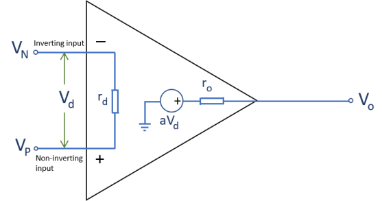
Practical operation amplifier model.

Key-part_1

Key-part_2


In an ideal operational amplifier (op amp), the value of rd is considered to be infinite when in actual fact the resistance is around 10MΩ. This value is dependent on the variety of omp amp and generally increases with price. The higher the value of rd, the better.

This same premise also applies to the open-loop gain. It’s value in an ideal op amp is also considered to be infinite, when in actual fact it is around 10M.

ro however is the inverse, as in an ideal op amp it is 0Ω and a typical practical value is about 10Ω,


Vout_formula

Using the above formula the following can be derived:

V difference formula

The difference between the voltage on the inverting input and the non-inverting input is equal to the output voltage divided by the gain.

Now assuming ideal values for the gain (infinite), its value can substituted in and the formula can be rearranged.

V difference formula (values)

Any value divided by infinity is equal to zero, therefore:

V difference formula (simp)

Looking back at the original formula, the following can be deduced:

Vout_formula (2)

Vout_formula (3)

Substitute in the value for Vd:

Vout_formula (4)

Rearrange:

Vout_formula (5)


In addition to this, two more values can be stated when using ideal values.

The value of rd is infinite, therefore no current is flowing into the inverting or non-inverting terminals (Ip = 0A and In = 0A).

The output impedance is 0Ω.


Semiconductor definitions/descriptions

Intrinsic and Extrinsic Semiconductors

Intrinsic

Intrinsic semiconductors are pure and undoped. They have an equal number of conduction electrons and holes. Thermal excitation is required for conduction.

Extrinsic

Extrinsic semiconductors are doped with impurity atoms, which generate majority carriers. The type of majority carrier is dependent on the dopant used. These are as follows:

N-type- Majority carriers are electrons, minority carriers and holes.

P-type- Majority carriers are holes, minority carriers and electrons.


Drift velocity of carriers

Drift velocity is the average velocity that a charge carrier, such as an electron, attains in a material due to an electric field.


Band-gap energy

The band-gap energy is the energy required to move an electron from the valence band to the conduction band.


Electron-hole recombination and the frequency of light emitted by an LED.

Electron-hole recombination

When an electron which has previously been excited from the valence, to the conduction band, falls back into an empty state in the valence band.

Frequency of light emitted by an LED

When an electron moves back from the conduction band to the valence band, energy equal to the band-gap energy is emitted.

This energy produces a frequency which is equal to the band-gap energy divided by Planck’s constant. In LEDs, the frequency produced is in the form of light (Hence the name Light Emitting Diode).

The chain rule

When trying to derive a composite function, we use the chain rule.

A composite function is a function that is comprised of two functions, one within the other. Here’s the generic formula:

chains

This shows the derivative of y with respect to x broken down into the derivative of y with respect to u multiplied by the derivative u with respect to x.

This is proven to be the same here:

proof-cr

The value of you can be substituted with whatever value is needed to derive the function. Here’s and example of the chain rule being used:

example-cr

…To be continued

dun dun dunnnnyuunjjnnnn

The product rule

When trying to derive a function that has two values multiplied together, we use the product rule.

This can be shown by the following formula:

product-rule

This simply shows that to derive u × v, you simply derive them separately. Once you’ve done this, you multiply each of these values by the others original value, and then add them together.

Here’s a worked example:

product-rule

Of course in this instance the product rule is not needed, and can also be solved the following way:

picture1

This does however prove that the product rule works, and In other instances, where the value cannot be simplified before deriving it, it is needed.

Stationary points

What is a stationary point?

Stationary points are where the gradient of a curve is equal to zero. They are divided up into three sub-groups: Maximums, Minimums, and inflection points.

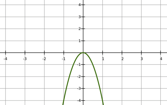
At a maximum point, the value of Y is always greater than the values of Y immediately before and after its position on the X-axis.

maximum

At a minimum point, the value of Y is always less than the values of Y immediately before and after its position on the X-axis.

minimum

At an inflection point, the value of Y is either greater than the value of Y immediately before it and less than the value of Y immediately after it, or the value of Y is less than the value immediately before it and greater than the Y value immediately after it.

inflection

Finding stationary points

First of all, you must find out if there are any stationary points in the line. To do this you differentiate the function.

For this example, we’ll use the following function:

funct1

Here it is shown on a graph:

sp1

As you can see, there are two stationary points (a maximum and a minimum). Normally, there wouldn’t be a visual aid, but for the sake of this example, corresponding graphs have been included.

SP2.png

Using your eye, you can roughly tell that the stationary points are at -1, and 3/2 on the x-axis. 

Now let’s go back to the algebraic function, and differentiate it.

funct1

funct2

Here’s the new term shown also shown as a graph:

graph_20161220_040635

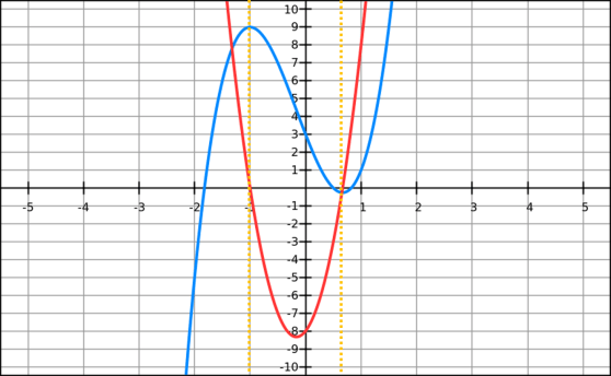
Now lets compare both of the functions together:

sp4

As you can see, the points at which the derived function have a Y value of 0, are also where the stationary points are on the original function. This is why the first step of finding stationary points, is finding the derivative of the function.

Now, back to the derived equation.

funct2

We must now set Y to equal zero, and then solve the quadratic.

quad1

Therefore at the stationary points, x equals:

quad2

Now we take these values, and substitute them back into the original function to find the Y coordinates:

funct1

stat1

Now we know that the stationary points on the curve are at the following coordinates:

stat2

Finding out what type of stationary point it is

Now that we know how to find the stationary points, we need to know what type of stationary point it is, without the aid of a graph.

To do this we first find the second derivative of the original function. This is represented by the following:

2nddr

All this is, is the derivative of the original function, differentiated again. Here’s the example we used:

funct1

funct2

2nddrrr

Now all we do is substitute the x values we found earlier into the formula.


drrrrrrrrrrrx

If the resulting number is:  

> 0    it is a minimum.

< 0    it is a maximum.

= 0     it is an inflection point.


Therefore at ( -1 , 9 ), there is a maximum, and at ( 2/3 , -7/27 ), there is a minimum.

Semiconductors

Overview

As the name suggests semiconductors are partially conductive materials, and lay somewhere between the conductivity of conductive metals and insulators.

N-type semiconductors

N-type semiconductors are generally composed of silicon, or germanium, doped in antimony. The doping provides a  free electron which increases the conductivity of the material.

The name derives from negative charge. This is because of electric current, where electrons break free from their atoms, and create a direction flow of electrons, with the aid of an electric field. Electrons flow towards vacancies in positively biased materials.

P-type semiconductors

P-type semiconductors are also generally composed of silicon, or germanium. However, Instead of being doped in antimony, they are doped in an element such as indium. This has the opposite effect to that of doping in antimony, as indium has a vacancy in its outer shell of electrons, to which a free electron can easily occupy.

The letter ‘P’ represents the fact that this material has a positive charge.

Conclusion

Under normal circumstances, In N-type semiconductors free electrons flow away from the materiel. Whereas In P-type semiconductors, free electrons flow towards the material to occupy the vacancies.

In terms of conventional current, current flows from P-type (positive) semiconductors, and current flows towards N-type (negative) semiconductors.

What is differentiation?

Differentiation is one of the two key components of calculus. It is the process of finding the derivative of a line. The derivative is the gradient of a tangent.

Without calculus, you can find the average rate of change by calculating the difference between two points. However, this only gives us a static unchanging gradient.

It’s quick, but it’s imprecise.When representing the gradient of a set of results with an average rate of change between two points, There’s no way to know what the line actually looks like between those points. To find that, we need to be able to find the gradient using only one point (a tangent instead of a secant line). By using only one point, we are able to find the instantaneous rate of change, rather than an average. This is differentiation.


What is slew rate?

The slew rate is the maximum rate at which the output voltage can change. This is especially relevant when amplifying sound waves using an op amp.

slew rate is the maximum change in voltage that can be achieved per second. The unit typically used is V/μs.

For example, a slew rate of 0.5 V/μs would be calculated using this formula:

2 x π x f x V = Slew rate (V/s)

So in this case you’d first convert 0.5 V/μs to 500 000 V/s.

Then to find the maximum voltage for a 1KHz signal you’d use this formula:

500 000/ (2 x π x 1000) = 15.71 volts.

This also means that a 1KHz signal can have an amplitude of 15.71 volts.

To put this into context, the human range of hearing is 20Hz to 20KHz. Therefore when amplifying audible sound you could have an amplitude of up to 3.98volts with this slew rate. Meaning that this op amp would be suitable for a 20KHz signal with an amplitude of 3.98 volts or less.

However when amplifying a 40KHz signal (a typical ultrasonic frequency), you’d only be able to achieve an amplitude of 1.989 volts. meaning that this op amp would only be suitable for 40KHz frequencies with an amplitude below 1.989 volts.


Capacitors in depth

Description

A capacitor is a component that has the potential to store an electric charge. Every capacitor is marked with two values: the capacitance, and the maximum voltage that it can be charged to.

The capacitance directly affects the charge and discharge rate of the capacitor. It’s unit of measurement are Farads (F), however capacitors that large are extremely rare, you’ll see the value marked in MicroFarads (uF) much more commonly. The larger the capacitance, the longer it takes to charge and discharge.

The charging time can be calculated by finding the value of the capacitor and the resistance of any components in series with the capacitor. However, because the charging time is not linear, it takes 5 times as long to get to approximately 100% capacity than it does to get to 63.2%.

The resistance multiplied by the capacitance equals the time it takes for the capacitor to charge to 63.2% of the supply voltage (RC= 0.632 x Vs).

Diode bridge

Overview

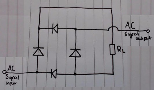
This is a diode bridge. It converts alternating current (AC), into direct current (DC). The circuit is set up so that current is always flowing towards the input of RL, and away from the output. More information about the properties of diode can be found here:’https://tphelectronics.com/2015/09/29/diodes/

ddone

AC signal output is most commonly just connect to ground (0v).

RL represents the circuit to which you’re applying the DC voltage.


Signal diagram explanation

dAC

This shows one full oscillation of the AC signal at the input. Whilst the signal is above the horizontal line, the voltage at the signal input is positive. Whilst the signal is below the horizontal line, the signal input is positive


Flow of current during positive half of the oscillation.

dACp

During the section labelled ‘Input is positive’, here’s how the current flows around the circuit:

dbp

The reason why the current can’t flow through D4, after passing through RL, is because D4 has already been reverse biased by current flowing from the AC input.


Flow of current during negative half of the oscillation.

dACn

During the section labelled ‘Input is negative’, here’s how the current flows around the circuit:

dbn


Conclusion.

As you can see, regardless of whether the AC input is positive or negative, the current flowing through RL never changes. If we could see what the current looked like at RL, It’d look something like this:

dCRL


Notes for future.

I’ll add in a diagram and explanation as to how to dampen the rippling effect seen in the graph above.